PCBA (Printed Circuit Board Assembly) manufacturing is a crucial step in the production of electronic devices. This process involves several intricate stages, each essential for creating functional circuit boards that power everything from smartphones to industrial machinery https://arisentecpcb.com/service/pcba/. In this article, we’ll explore the various aspects of PCBA manufacturing, from its fundamentals to the latest trends.
Understanding PCBA Manufacturing
1. PCB Fabrication
PCB (Printed Circuit Board) fabrication is the initial step in PCBA manufacturing. It involves designing and creating the actual board that holds the electronic components. Here’s how it works:
- Design: Engineers use CAD (Computer-Aided Design) software to design the PCB layout, specifying the placement of components and routing of electrical connections.
- Substrate Selection: The choice of substrate material (usually fiberglass-reinforced epoxy) depends on factors like durability, heat resistance, and cost.
- Layering: Most PCBs are multi-layered, with conductive layers separated by insulating layers (dielectric).
- Copper Cladding: Copper is applied to the substrate using a process called etching or deposition, forming the conductive pathways.
2. Component Procurement
Once the PCB is fabricated, components are sourced and prepared for assembly:
- Component Selection: Manufacturers choose components based on specifications (size, power ratings, tolerances) and compatibility with the design.
- Sourcing: Components are sourced from suppliers worldwide, ranging from basic resistors and capacitors to advanced microprocessors and ICs.
- Quality Assurance: Strict quality controls ensure that components meet specifications and are authentic (free from counterfeiting).
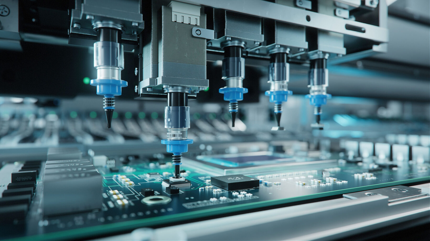
3. PCB Assembly
PCB assembly involves placing and soldering components onto the board:
- Component Placement: Automated machines or sometimes manual labor place components onto the PCB according to the design.
- Soldering: Solder paste, a mixture of flux and solder particles, is applied to the PCB. Components are heated, melting the solder and creating electrical connections.
- Inspection: Automated optical inspection (AOI) and X-ray inspection check for defects like misalignment or solder bridges.
4. Testing and Quality Control
Once assembled, PCBAs undergo rigorous testing:
- Functional Testing: Ensures the PCBA performs as expected under normal operating conditions.
- In-Circuit Testing (ICT): Tests specific electrical characteristics and verifies component values.
- Environmental Testing: PCBAs may undergo thermal cycling, vibration testing, and other stress tests to ensure reliability.
Trends and Innovations in PCBA Manufacturing
1. Industry 4.0 Integration
- Automation: Increasing use of robotics and AI-driven systems for assembly and quality control.
- IoT Connectivity: PCBs are increasingly IoT-enabled, capable of transmitting and receiving data for smart applications.
2. Miniaturization and Advanced Materials
- Smaller Form Factors: Demand for smaller, lighter devices drives miniaturization of components and PCBs.
- Flexible and HDI PCBs: High-Density Interconnect (HDI) PCBs and flexible PCBs cater to applications needing compact, bendable designs.
3. Green Manufacturing
- Lead-Free Manufacturing: Compliance with RoHS (Restriction of Hazardous Substances) regulations.
- Energy Efficiency: Efforts to reduce energy consumption during manufacturing processes.
PCBA manufacturing is a complex, evolving field critical to the electronics industry. As technology advances, the demand for smaller, faster, and more reliable PCBAs grows. Manufacturers must innovate continuously to meet these demands while maintaining high standards of quality and efficiency.